Solar Charger And Inverter
SAGI Universe
July 2020
Back
1.Introduction
DIY projects often originate from the needs of your daily life. In our case, we have a shed in the garden that is not connected to the house and does not have electricity. During the night, we wanted to have a light inside the shed, where we do small works and light outside that switches on in darkness. Besides, in our storage, we had a second-hand 50W solar panel, bought at a scrape yard sale, a few 12V 10 Ah batteries recycled from a broken UPS, and a large supply of new or recycled electronic components, including 10- 20 VA transformers. Therefore, we have decided to build a mini-system for storing energy during the day and use it during the night to provide illumination using these reclaimed materials.
That is why we have named this project solar charger and inverter: SCI. It charges a battery based on a solar array and produces 220V AC voltage for supplying standard LED lamps.
Nothing new, you can rightly say, indeed you can buy cheap modules and assemble them to provide this function. But can you repair them if they get broken? The answer is no, most of the time the control board is made using SMD parts and the whole mechanical assembly breaks into pieces when you try to disassemble them. Also, where is the fun of designing and building the functions?
2.SCI System targets
The main objectives for the SCI system have been:
● AC power output: 20-25 W, enough to power at least 2 LED lights.
● AC sine wave, so that it can also charge electronics using the generated power. In commerce, you find either sinusoidal AC inverters, the most expensive, or the cheaper quasi-sinusoidal or just square-wave inverters. With these last ones, not only can you not supply sensitive electronics but also some LED lights do not switch-on.
● Built-in protection for battery surcharge (to avoid overheating of the battery).
● Transformer isolation between the low voltage (12V) generation section and the 220V output section. This allows a safer building and testing of the device, but also the possibility to connect at the 220V output a differential residual current breaker to protect from electric shock.
● Automatic switch-on of the AC power at night.
● Interface for a remote telemetry transmitter, to be able to monitor the system performance wirelessly.
● Potential expandability of the design for higher AC output power (50 – 100 W).
● Connection to a potential back-up charging source (for example, a wind electric generator).
● Maximum re-use of recycled hardware and components.
For the design, we have used the following open-source or free tools:
● MikroC compiler (ref.1) for Microchip MCUs. This has a design limit that is not a problem for the project described in this post. However, if you want more optimized executables and no limitations, a paid version is available that costs between 200 and 250 Euro.
● LTSpice (ref.2) for DC/AC simulation.
● QUCS (ref.3) and/or QUCS Studio (ref.4) and/or QUCS-S (ref.5) for output filter and ADC input simulation.
● KiCad (ref.5) for PCB design.
● Octave (ref.6) for various math calculations and also for serial data plotting.
All of them run on MAC Pro except the MikroC compiler. For this, a VirtualBox with Windows7 can be used.
3.Design
There are many papers on the subject of generating AC power from solar panels and batteries, from them we can deduce that the following main strategies are possible:
● A DC-DC converter to transform the voltage from the solar array(s) to a voltage close to the AC (rms) output voltage, and then a conversion from DC to AC.
● A DC-AC converter working to the solar panel/battery voltage followed by a transformer to elevate the voltage to the output AC voltage.
The first solution is what is often used in solar-panel installations without accumulation (i.e. no local energy storage in batteries) as it allows us to avoid an output transformer and to be able to reach higher powers. This was not the optimal approach for this project and therefore we opted for the second solution.
The schematic of the basic building blocks for the adopted solution, as implemented, is indicated in figure 1.
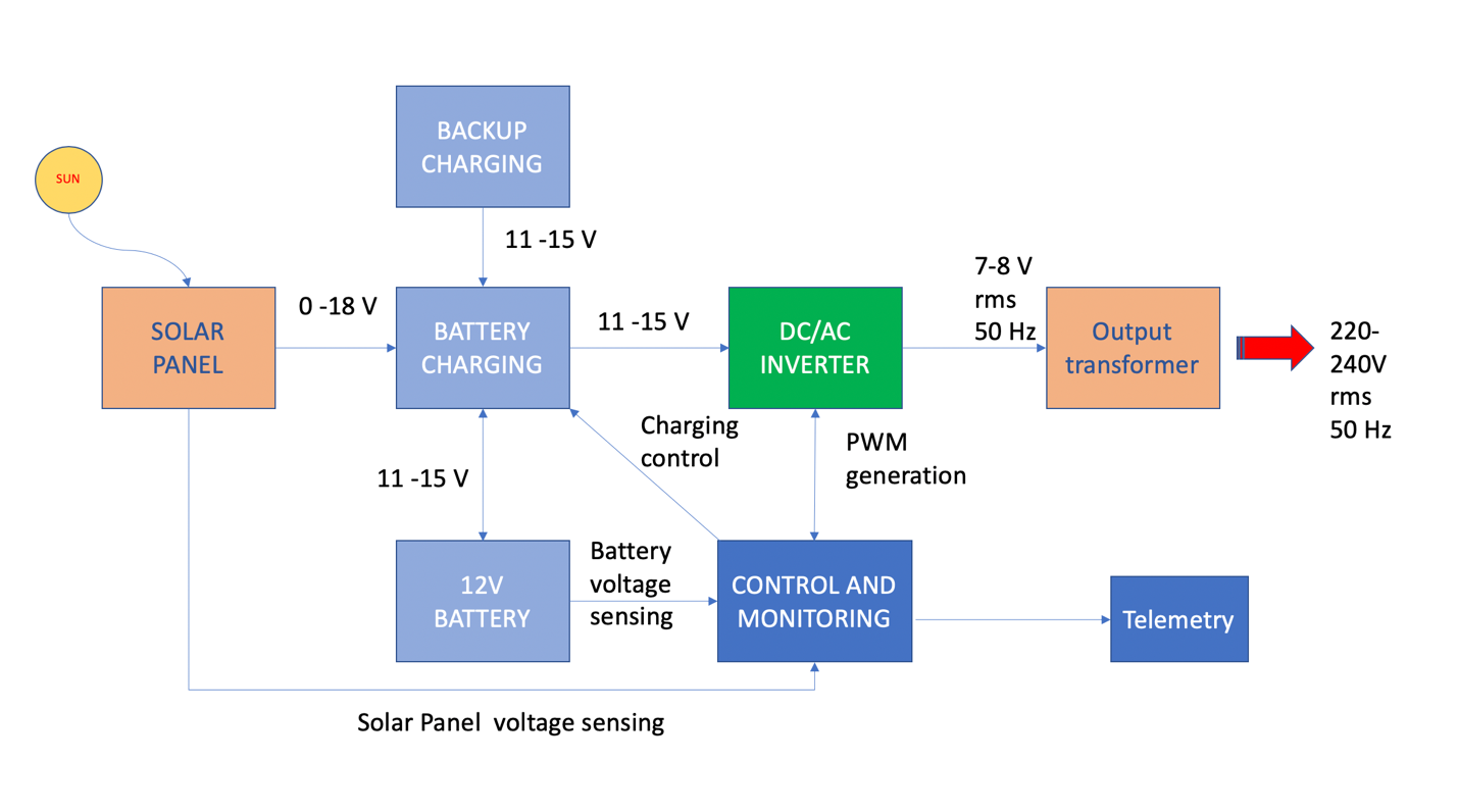
Figure 1 -SCI block diagram
3.1 Control and monitoring block
The core of this function is the control and monitoring unit. This is made using a microcontroller that should be able to monitor the battery and solar panel, control the battery charging, generate the Pulse Width Modulation (PWM) signals for the inverter and provide the interface for a remote telemetry interface. The first thought could go to an Arduino board with a few dedicated shields. However, for this SCI, we prefer to use more lower-level functions and implement them directly. Therefore, we have chosen to use a Microchip microcontroller (MCU) that can implement all the functions depicted in figure 1: ADC for voltage sensing, PWM for driving the DC/AC converter, and a serial interface for the telemetry interface. we have selected a PIC 16F690 device (ref.8) in DIL package (for easy assembly and replacement in case of failure) for the purpose.
3.2 DC/AC Block
Concerning the DC/AC converter, this is implemented with a full H-bridge using MOSFET devices.
The full H-bridge arrangement is shown in figure 2 (taken from the PIC 16F690 datasheet, ref.8).
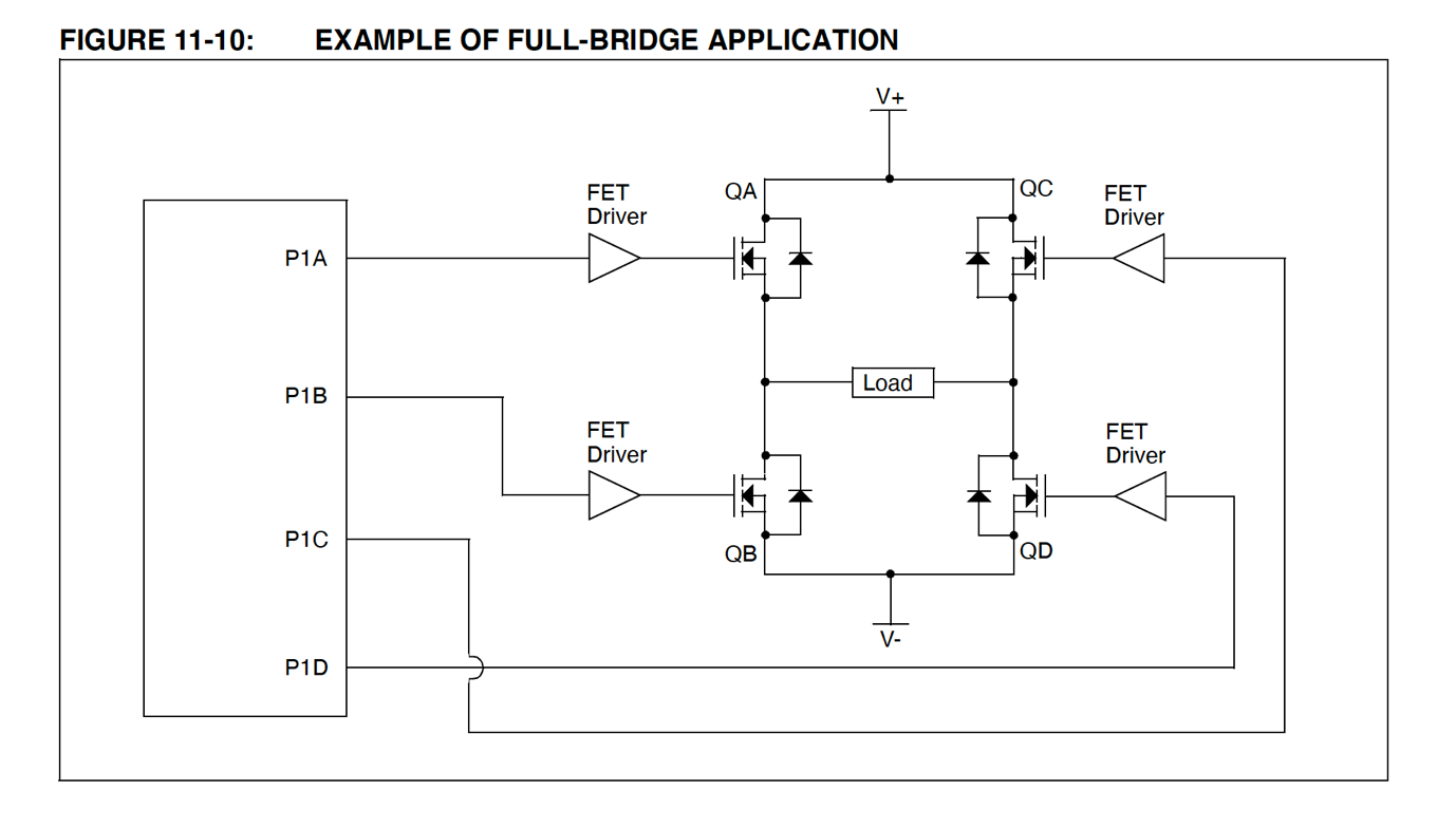
Figure 2 – Full H-Bridge configuration
The MCU supplies the bridge with full PWM signals through the four outputs P1A, P1B, P1C, and P1B.
This bridge utilizes four N-Type MOSFETs. The devices should be driven by a voltage higher than the one provided by the PIC device (typically 7-8 V Vgs) and, in particular, the MOSFET on the top of the H-bridge, have a floating source and therefore the voltage to be applied to the gate of these devices shall be even higher (typically 19-20 V). Therefore as these voltages cannot be generated by the PIC, a driver should be inserted between the PCI and the MOSFET. You can use for example two IR2110 devices. This IC with have a bootstrap function that is able to generate, with the help of an external capacitor and a diode, the higher voltage necessary for the “high” MOSFETs.
In alternative, P-type MOSFETs can be used for the high-side of the bridge and in this case the circuit simplifies as you can use a single quadruple drive such as the SN754410. We have chosen this simpler option. The disadvantage is that P-type MOSFETs have an higher RDS value than N-type and therefore you may want to use this only for more limited inverter output power.
The MCU generates a pseudo sinusoidal wave by modulating the pulse width of the PWM signal according to a simulated sine-wave table. This is presented in figure 5, with a simulation performed in Octave. The top drawing shows the PWM waveform modulated by the absolute value of a sine wave. The bottom part displays the control signal to the two branches of the H-bridge (top left and bottom right MOSFETs and top right and bottom left MOSFETs). When the first branch is active the PWM signal is generated for the positive part of the sine-wave. The negative part is produced when the second branch is active.
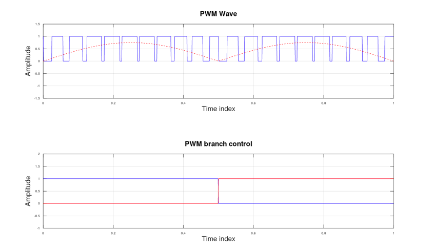
Figure 3 - PWM modulated by a sine wave
The PWM frequency shall be as high as possible compared to the desired sinusoid frequency, in this case, 50 Hz, to facilitate filtering. The PIC 16F690 with a clock frequency of 8 MHz could easily generate a PWM with a frequency of up to 200 kHz. However, the higher the PWM frequency, the higher will be the switching losses and, in addition, the resolution of the PWM generation will decrease. We have chosen a PWM frequency of 20 KHz and this, according to the formulas included in ref.1, gives a resolution of 8 bit.
The load in the H-bridge is not directly the primary of the output transformer, but a network is inserted between the H-bridge and the load. First, a coarse filtering constituted by two inductors and a capacitor, is inserted between the bridge outputs and the transformer. This network includes also a resistor to load the transformer and reduce spikes.
Then, the main filtering is provide by adding a capacitor and another internal resistive load at the output of the transformer. This load is necessary to avoid excessive voltage and dissipation when there is not an external load and the solar panel is in full illumination. If the inverter is used for constant loading this internal load can be removed, saving a few watts.
The filtering action has been simulated using QUCS Studio and you can see the effect on a square wave input signal.
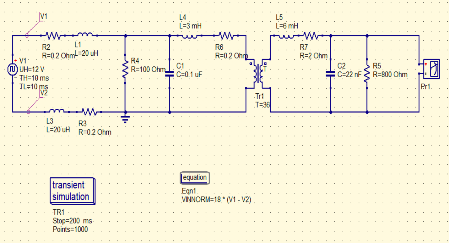
Figure 4 - Overall output network
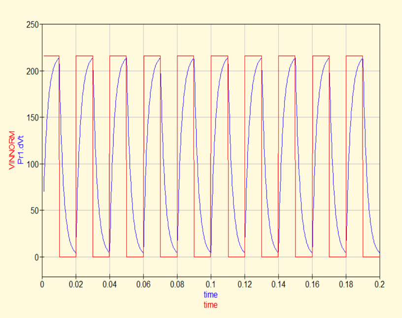
Figure 5 - Smoothing effect on a square wave
Concerning the transformer, you should choose one with a power rating (in VA) compatible to your application. We have tried with several recycled transformers, with a input winding for an AC voltage of 6 to 9 V and an output winding for 220 V, with power (judged from the size) from 20 VA to 100 VA. In our experience, if you want a continuous power at the output of the inverter of 50 W you should choose a transformer with at least 75 to 100 VA capability to avoid saturation of the magnetic core (and consequent higher dissipation and failure of the inverter).
3.3 Charging function
The solar panel voltage and the battery voltage are monitored by the MCU using two of the available 10 bit Analog to Digital Converters (ADCs). As the input voltage to these ADCs will be limited to the MCU positive supply value (in this case Vdd = 5 V), both the solar panel and battery voltages are reduced with a resistor divider by 5, implemented with two resistors. The relevant input pins of the MCU are also protected by a 5.1 V Zener diode to avoid failures for excessive input voltages, and a 470 uF capacitor filters potential interferences coming from other parts of the circuit. This high value is compatible with this application as the change of voltages is inherently at slow rate.
Once the solar panel and battery voltage are measured by the ADCs, the MCU compares them and performs a suitable action according to the comparison between the two.
If the battery is overcharged (more than 14.5 V), the solar panel voltage supply is short circuited by a N -type MOSFET. Note that short-circuiting a solar panel does not damage it.
Besides, the solar panel voltage value is also used to detect the transition to darkness: if the voltage is below 1 V, the DC/AC converter is activated and the 220V output voltage is present then the connected lights are activated. Above 1 V, only the charging function is active. This feature can be deactivated if not necessary (i.e., you want to use the energy generated by the solar panel also during the day).
3.4 Other circuit parts
The solar panel utilised has a short circuit current of about 3.5 A and an open circuit voltage of up to 22V, in full illumination. It is connected to the SCI through a 6.3 A fuse, for protection especially during testing, and by a low-drop Schottky diode (to avoid current to flow from the battery to the panel when the panel voltage is low, which would damage it).
Concerning the output transformer, we have used a recycled 8-220V 10 VA standard transformer. For higher power, toroidal transformers can be used.
Also, the battery is connected to the SCI through a fuse. Here you should use a 10 A fuse or a delayed lower amperage fuse to cope with the transient when you connect the battery to the unit. The backup voltage source is also protected by a fuse and connected to the battery through a Schottky diode. If you install an SCI in a place where the home 220V voltage is available, then you could use a 12-13 V 1A reclaimed charger that will be used only when the battery voltage is low and the solar panel does not produce sufficient energy to keep the battery charged. This is implemented with a switch based on a P-type MOSFET.
Concerning the effectiveness of using the solar panel to charge a battery, in the implementation chosen for the SCI the panel is always directly connected to the battery. It is clear that a more efficient use would be through the use of a Maximum Power Point Tracking (MPPT) algorithm. This would maximize the solar panel capability to charge the battery, by modifying the voltage applied to the battery using a buck DC/DC converter or a combined buck-boost DC/DC converter. This, of course, would increase significantly the complexity of the SCI but we will considered this in future developments.
3.5 Telemetry Interface
In some cases, it is interesting to be able to check the SCI remotely. This can be done either using the USART interface available in the PIC 16F690 or using an external telemetry unit that gets information from SCI (for example, voltages, status bits). This will be the subject of another post.
3.6 MCU Firmware
The block diagram of the firmware is shown in figure 8:
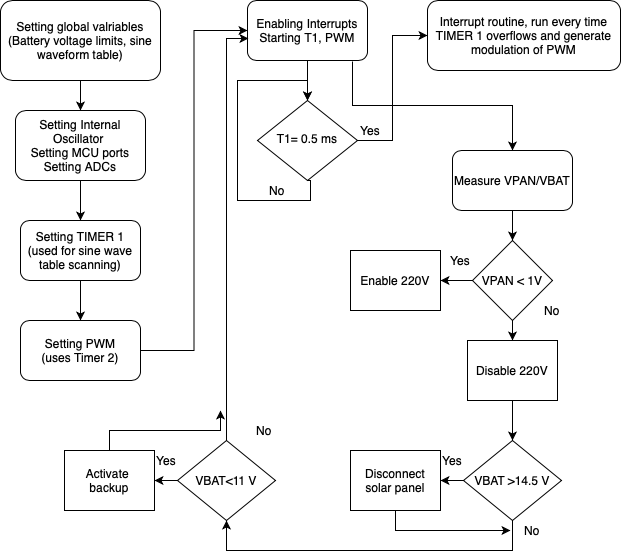
Figure 6 - Firmware flowchart
The firmware starts, in a dedicated subroutine, by setting the global variables (battery limits, the PWM sine-wave table). The table has 20 entries for a half sinusoid (as the second half is identical to the first half: the only difference is that the first half is used to drive the first branch of the H-bridge and the second half – the same table – is used to drive the second branch of the H-bridge). Therefore, to get a 50 Hz PWM waveform (20 ms period), a sampling time of the half sinusoid of 10 ms / 20 = 0.5 ms is needed.
Then the firmware sets the MCU internal oscillator to 8 MHz and initializes the MCU relevant ports to input or outputs, as needed, the ADC ports are selected and the ADC conversion settings are assigned.
After this, the MCU timer 1 is set for a cycle of 0.5 ms for changing the PWM waveform according to the sine table.
The MCU timer 2 is then set to provide a PWM of 20 kHz.
Following the settings routine, the interrupt routine is defined. This routine is initialized every time the timer 1 overflows as it reaches 0.5 ms, and scan through the sine-wave table to provide a quasi-sinusoidal PWM waveform.
The Main routine is then defined, starting with setting the initial values of the variables (for example setting to zero the pointer to the sine-wave table) and then enabling the Timer 1 and Timer 2. Then, the ADC for the solar panel voltage and the ADC for the battery voltage are cyclically run for measuring these voltages and the measured voltages are compared with the reference values to decide if to enable the 220V generation, or disconnect the solar panel (see figure 8). In addition, there is a duty cycle compensation routine that adjust the average duty cycle according to the battery voltage, to ensure a reduced variation of the 220 V.
4.Final Circuit
The final circuit schematic of the SCI is shown in figure 9, using the circuit diagram capability of KiCad. In the circuit, you can see a few details not described above.
There is a 5V regulator to provide the MCU with regulated Vdd from the battery. The circuit with an N-MOSFET in the bottom left corner is responsible for short circuiting the solar panel input (this does not damage the solar panel) in case of battery over-charge. Just of the left of this MOSFET, you can notice that we have used two Schottky diodes in parallel between the solar panel and the battery to reduce to the minimum the losses due to the diode barrier and resistance.
The P-type MOSFET on the top right corner connects or disconnects the backup charging source, if present.
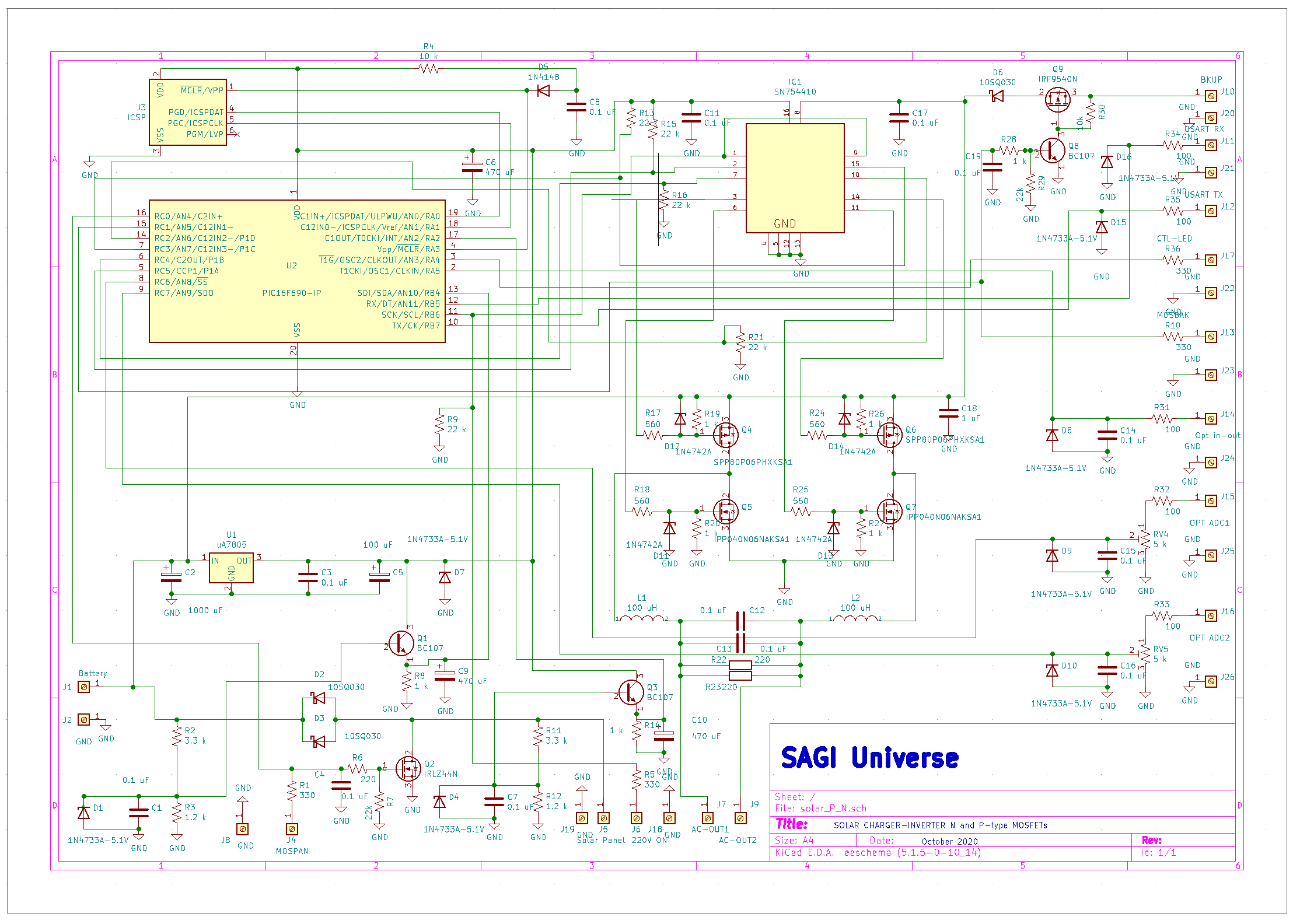
Figure 7 - Final SCI schematic – P&N MOSFETS
On the right side, we have foreseen optional inputs for further expansion (for example, additional measurements, such as the battery temperature, or implementing a differential current switch using a differential coil for the 220 V output).
Input J13 and J14 can also be utilized to access the MCU UART for serial communication.
J4, J6, and J12 are interfaces where you can connect LEDs to monitor the status of the 220V enabling function, the solar panel shorting functions and the backup enabling function.
Concerning the component choice, with the exception of the MCU and the MOSFET driver IC, there is quite a flexibility to use, for example, MOSFETS different from those indicated in the schematic. As a rule of thumb, use MOSFETs with twice the voltage and current capabilities, compared to those required in your application. In addition, make sure that also the maximum gate-source voltage rating is more than 12 V (20 V, for example).
Other limiting factors are the transformer power capability, the Schottky diodes current capabilities and also the current limitations of narrow copper traces, if you use a PCB.
5.Implementation and Testing
We initially built test model of the unit on one solderless test breadboard for checking functionalities and finalizing the firmware.
All the MOSFET should be mounted on the heatsink (we have used in our case the body of the metallic box very effectively).
we also recommend that for the first switch on you do not connect the transformer to the H-bridge outputs. Just check with an oscilloscope that you get the expected waveforms.
For testing the unit, we have used two laboratory power supply to simulate the solar panel and the battery. The load has been simulated with an own built test box containing 100W resistors that can provide a simulated load from 10 to 150 W at 220 V.
Then we built a first engineering model style unit using a recycled metallic box (figure 10).
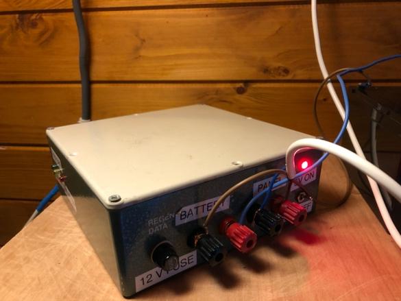
Figure 11 - SCI Engineering Model
This unit has been installed in our shed (figure 11, 12, 13) and has operated continuously for more than 6 weeks, to date.
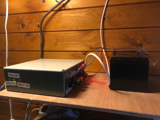
Figure 12 - SCI connected to battery and solar panel
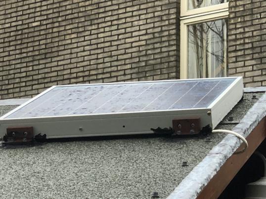
Figure 13 - Solar Panel mounted on shed's roof using 3D printed brackets

Figure 14 - SCI in action
We have then designed a box for a second engineering model and built the box using our 3D printer. This unit has been connected with a 100W solar panel. We then built two more units for an installation in our vacation location.
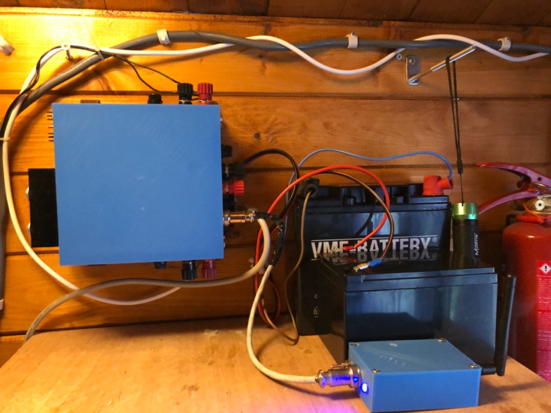
Figure 15 - Second engineering unit

Figure 16 – 100 W panel on the side of the 50 W panel
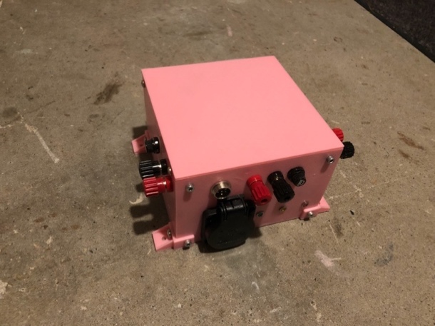
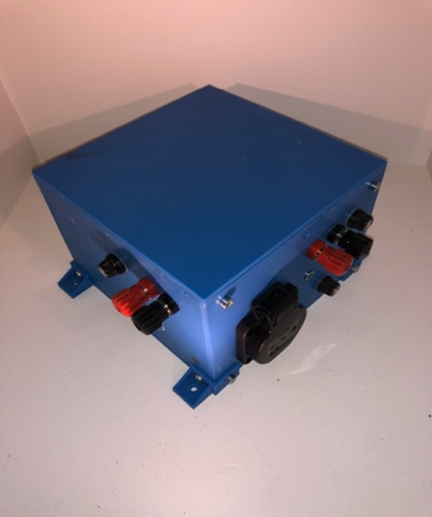
Figure 17 - Third and fourth unit built
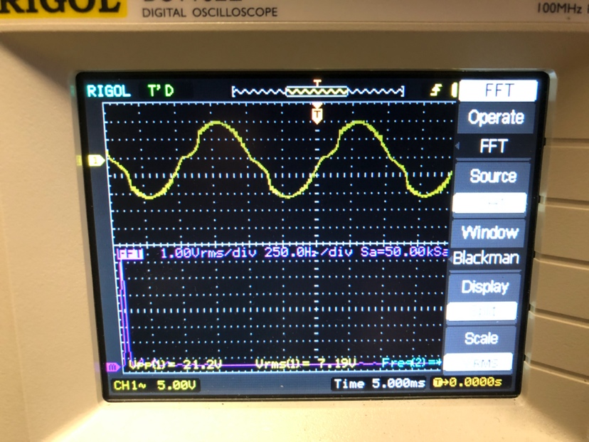
Figure 18 – Output voltage and spectrum
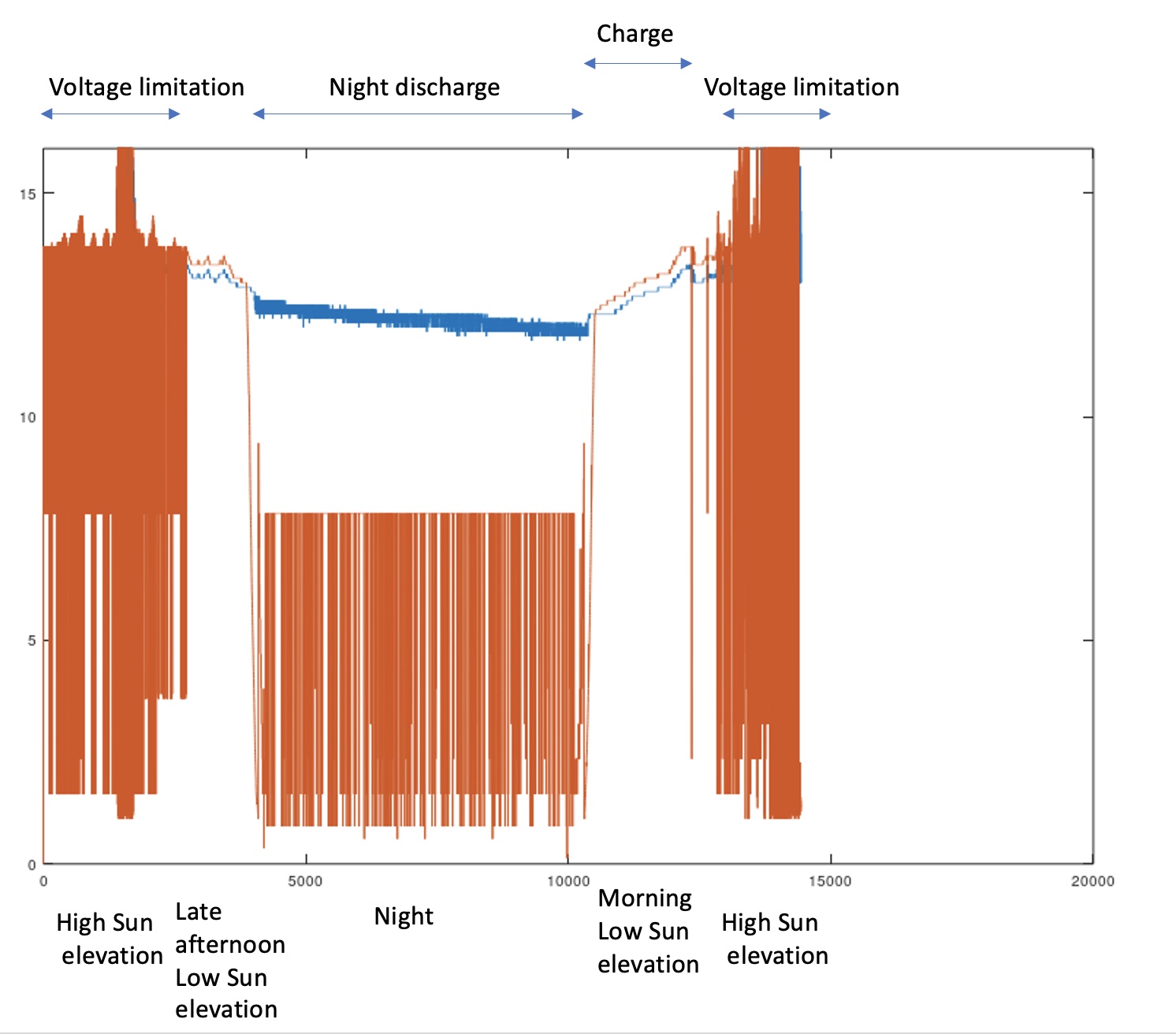
Figure 18 – Battery voltage and Solar Panel Voltage over one day: showing charging behaviour, over voltage control and discharging
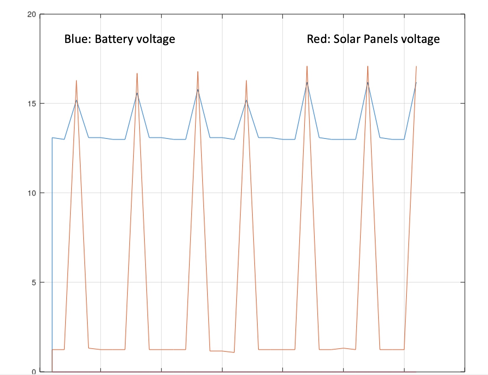
Figure 19 – Battery voltage protection details
6.Summary Performance
- Rated output power: 30 W (depends on transformer)
- Input voltage: 11.5 V – 14.5 DC
- Output voltage: 220VAC ±15%
- Output frequency: 50Hz ±5 %
- Efficiency (full load): > 85%
- Converter on - no-load current: <0.5A @ 12 V
- Converter off current: <0.05A @ 12 V
- Output waveform: sine wave (20 points sampling per half-wave)
- Automatic night function (if activated)
7.Recommendations
Be careful with the 220V!!!
Do not disconnect the battery with full load: arcs can be generated!!!
Connect a differential ground fault breaker in series between the 220V and the load to protect you from electric shocks.
Always use fuses (battery line, solar panel line and backup source line) for protecting the circuit and yourself!
8.Disclaimer
This circuit generate a dangerous AC voltage at 220V.
Therefore, you can use the content of this background document at your own risk. SAGI Universe cannot accept any responsibility for any injuries or damages from the use of the content of this post.
The information contained in this paper is for educational and informational purposes only, and is made available for the reader's own use.
9.References
- https://www.mikroe.com/mikroc-pic
- https://www.analog.com/en/design-center/design-tools-and-calculators/ltspice-simulator.html#
- https://github.com/Qucs/qucs/blob/qucs-0.0.19/NEWS.md
- http://dd6um.darc.de/QucsStudio/qucsstudio.html
- https://ra3xdh.github.io/
- https://kicad-pcb.org
- https://www.gnu.org/software/octave/
- https://www.microchip.com/wwwproducts/en/PIC16F690
- http://www.ti.com/lit/ds/symlink/sn754410.pdf
Back